Yale Electron Microprobe & SEM Laboratory
 The Yale Microprobe Facility
The Department of Earth and Planetary Sciences
and The Earth Materials Characterization Center (EMC^2)
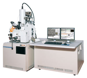
The Yale University microprobe facility houses a JEOL JXA-8530F (FEG) "Hyperprobe" - electron probe microanalyzer (EPMA; aka electron microprobe analyzer, EMPA) - installation of which began in April 2009. This EPMA/SEM functions with state-of-the-art imaging, analytical, and computer-control capabilities. This probe configuration includes five wavelength-dispersive spectrometers (WDS) and a light-element-capable energy-dispersive spectrometer (EDS) with Windows-7 processing software. Hardware and software allow automated operation and data collection, and software accommodates advanced image processing and feature analysis. Additional instrumental details can be accessed here. This lab also includes a turbo-pumped Emitech carbon evaporator/coater, which also includes metal evaporation capability. Jim Eckert is available to answer questions and assist users with all forms of analysis. For information on instrument access, click here. Current hourly usage rates are available here.
We invite your interest in our electron microprobe/SEM facility. For more information, please contact Jim Eckert. With this system we are able to acquire data with the native JEOL interface. We also can acquire WDS quantitative and qualitative/wavescan data with the Probe-for-EPMA software (probewin.exe) we used previously with the JXA-8600.
USES OF THE MICROPROBE, 1. IMAGING:
Since the microprobe functions also as a scanning electron microscope (SEM), in addition to element maps of a specimen, images from secondary electrons (SEI) and back-scattered electrons (BSE, a.k.a. COMPO or BEI) also can be produced. The Yale JXA-8530F rivals or surpasses most SEMs in the ability to resolve detail and represent with clarity the textural relationships in a specimen. This capability, coupled with the quantitative analysis described below, permits detailed microscale to nanoscale assessment of a specimen. SEM imaging with the 8530F can routinely apply magnifications over 250,000X.
USES OF THE MICROPROBE, 2. MICROSCALE CHEMISTRY:
QUALITATIVE ANALYSIS
Qualitative and semi-quantitative microscale chemistry can be assessed rapidly using EDS spectrometry. This can benefit phase identification and recognition of compositional variability in a sample. This allows rapid imaging and compositional mapping, as well as storage of images and data in readily transferable formats. With either the native JEOL acquisition software or with Probe for Windows, we also can accommodate integration of EDS data into the quantitative-analysis package.
QUANTITATIVE ANALYSIS
Quantitative microscale chemical analysis, using wavelength dispersive spectrometry (WDS), requires both a stable, well-tuned instrument and standards for comparison that are both well characterized and appropriate for a given specimen. The JXA-8530F is proving to be a stable instrument most of the time, and the Yale suite of available standards is quite diverse and extensive. Typical operating conditions for the electron beam are an accelerating voltage of 15 kV beam currents of 5 to 20 nanoamps, and beam diameter of 1 to 10 microns. However, these parameters can be varied widely (0.5 - 30 kV, ~10 pA to ~1500 nA, beam diameter from focused to ~30 microns {maximum for spectrometer focusing geometry}) to address various questions. Many of the Yale standards, a collection begun by Horace Winchell in the 1960's, are appropriate representatives of their mineral group. These generally high quality standards, which include both synthetic and naturally occurring varieties, have been graciously provided by a wide variety of esteemed scientists over several decades. Nonetheless, alternative standards for less traditional projects also can be applied.
Quantitative analysis can address all elements heavier than beryllium (boron and higher). Each analysis takes several minutes to count the X-rays and perform related calculations. Ultimate WDS detection limits for sodium and heavier elements are about 50 to 100 ppm (0.005 to 0.01 wt%, elemental); for lighter elements, the instrument is somewhat less sensitive. For most major elements, these truly quantitative microscale chemical measurements typically have accuracy and precision on the order of 1%. Comprehensive setups applied heretofore include a 33-element oxide setup, incorporating all REE with overlaps and interferences. Automated analysis allows the operator to assign locations for analysis during a session, then acquire data automatically (unattended) at those stored locations. Thus, the operator may concentrate on other tasks while the time-consuming X-ray counting and data reduction are completed. Data can be transferred via network or USB connections for rapid accommodation into reports and manuscripts.
APPROPRIATE SPECIMENS
Appropriate specimens for microprobe imaging and analysis can be geological, biological, or technical materials of various compositions and textures. To be appropriate, specimens must be:
- solid and dry with a clean surface
- stable in a vacuum and under a high-voltage electron beam (some less
stable materials can be evaluated under less intense voltage and
current, though this limits quantitative potential)
- polished on the flat upper surface (for quantitative analysis) - this
can be completed in the lab here, if needed
- mounted on either:
1) 25.4 mm (1") diameter cylindrical blocks, plates, or discs;
2) 27 mm wide (standard petrographic {U.S.}) glass slides or thin (~1 mm) plates up to 80 mm long (45 mm standard);
3) another substrate no more than 100 mm X 100 mm and 25 mm thick (high)
- able to conduct an electrical current or to be coated with a thin layer of
conductive carbon (coating ideally performed in the lab here).
USES OF THE MICROPROBE, 1. IMAGING:
Since the microprobe functions also as a scanning electron microscope (SEM), in addition to element maps of a specimen, images from secondary electrons (SEI) and back-scattered electrons (BSE, a.k.a. COMPO or BEI) also can be produced. The Yale JXA-8530F rivals or surpasses most SEMs in the ability to resolve detail and represent with clarity the textural relationships in a specimen. This capability, coupled with the quantitative analysis described below, permits detailed microscale to nanoscale assessment of a specimen. SEM imaging with the 8530F can routinely apply magnifications over 250,000X.
USES OF THE MICROPROBE, 2. MICROSCALE CHEMISTRY:
QUALITATIVE ANALYSIS
Qualitative and semi-quantitative microscale chemistry can be assessed rapidly using EDS spectrometry. This can benefit phase identification and recognition of compositional variability in a sample. This allows rapid imaging and compositional mapping, as well as storage of images and data in readily transferable formats. With either the native JEOL acquisition software or with Probe for Windows, we also can accommodate integration of EDS data into the quantitative-analysis package.
QUANTITATIVE ANALYSIS
Quantitative microscale chemical analysis, using wavelength dispersive spectrometry (WDS), requires both a stable, well-tuned instrument and standards for comparison that are both well characterized and appropriate for a given specimen. The JXA-8530F is proving to be a stable instrument most of the time, and the Yale suite of available standards is quite diverse and extensive. Typical operating conditions for the electron beam are an accelerating voltage of 15 kV beam currents of 5 to 20 nanoamps, and beam diameter of 1 to 10 microns. However, these parameters can be varied widely (0.5 - 30 kV, ~10 pA to ~1500 nA, beam diameter from focused to ~30 microns {maximum for spectrometer focusing geometry}) to address various questions. Many of the Yale standards, a collection begun by Horace Winchell in the 1960's, are appropriate representatives of their mineral group. These generally high quality standards, which include both synthetic and naturally occurring varieties, have been graciously provided by a wide variety of esteemed scientists over several decades. Nonetheless, alternative standards for less traditional projects also can be applied.
Quantitative analysis can address all elements heavier than beryllium (boron and higher). Each analysis takes several minutes to count the X-rays and perform related calculations. Ultimate WDS detection limits for sodium and heavier elements are about 50 to 100 ppm (0.005 to 0.01 wt%, elemental); for lighter elements, the instrument is somewhat less sensitive. For most major elements, these truly quantitative microscale chemical measurements typically have accuracy and precision on the order of 1%. Comprehensive setups applied heretofore include a 33-element oxide setup, incorporating all REE with overlaps and interferences. Automated analysis allows the operator to assign locations for analysis during a session, then acquire data automatically (unattended) at those stored locations. Thus, the operator may concentrate on other tasks while the time-consuming X-ray counting and data reduction are completed. Data can be transferred via network or USB connections for rapid accommodation into reports and manuscripts.
APPROPRIATE SPECIMENS
Appropriate specimens for microprobe imaging and analysis can be geological, biological, or technical materials of various compositions and textures. To be appropriate, specimens must be:
- solid and dry with a clean surface
- stable in a vacuum and under a high-voltage electron beam (some less
stable materials can be evaluated under less intense voltage and
current, though this limits quantitative potential) - polished on the flat upper surface (for quantitative analysis) - this
can be completed in the lab here, if needed - mounted on either:
1) 25.4 mm (1") diameter cylindrical blocks, plates, or discs;
2) 27 mm wide (standard petrographic {U.S.}) glass slides or thin (~1 mm) plates up to 80 mm long (45 mm standard);
3) another substrate no more than 100 mm X 100 mm and 25 mm thick (high) - able to conduct an electrical current or to be coated with a thin layer of
conductive carbon (coating ideally performed in the lab here).